Proper PCB Design for Assembly: Best Practices for Efficient and Reliable Electronics Manufacturing
The success of any electronic product depends not only on circuit functionality but also on how easily and efficiently the design can be manufactured. Even the most innovative circuit can face production delays, increased costs, and reliability issues if the board is not designed with assembly requirements in mind. This is why Proper PCB Design for Assembly is one of the most important considerations in modern electronics development.
As electronic devices become smaller, more complex, and more feature-rich, manufacturers increasingly rely on Design for Manufacturability (DFM) principles to ensure smooth production. Proper PCB Design for Assembly helps reduce manufacturing defects, improve production efficiency, lower costs, and enhance long-term product reliability. Understanding these design principles is essential for engineers, product developers, and businesses involved in electronics manufacturing.
What Is Proper PCB Design for Assembly?
Proper PCB Design for Assembly refers to the practice of designing printed circuit boards in a way that simplifies component placement, soldering, inspection, testing, and overall manufacturing processes.
Rather than focusing solely on electrical functionality, designers must also consider how the board will be assembled on the production line. This includes evaluating component placement, pad design, routing, spacing, panelization, testing access, and manufacturing tolerances.
By incorporating assembly requirements during the design phase, manufacturers can minimize production challenges and improve product quality.
A board that is easy to assemble generally results in fewer defects, faster production times, and lower manufacturing costs.
Why Proper PCB Design for Assembly Matters
Manufacturing issues often originate during the design stage. Poor design choices can lead to component placement errors, soldering defects, inspection difficulties, and increased production expenses.
Proper PCB Design for Assembly offers several important advantages:
- Reduced manufacturing defects
- Improved assembly efficiency
- Lower production costs
- Faster time to market
- Better product reliability
- Higher production yields
- Simplified testing procedures
These benefits make assembly-oriented design an essential part of successful electronics manufacturing.
Companies that prioritize manufacturability early in development often experience fewer production delays and lower overall project costs.
Understanding Design for Manufacturability
A key aspect of Proper PCB Design for Assembly is Design for Manufacturability, commonly known as DFM.
DFM involves designing products in a way that simplifies manufacturing while maintaining performance requirements.
For PCB assembly, DFM focuses on ensuring that components can be placed accurately, soldered reliably, inspected effectively, and tested efficiently.
Manufacturers often perform DFM reviews before production begins. These reviews identify potential issues that could impact assembly quality or increase manufacturing costs.
Addressing DFM concerns early helps prevent costly design revisions later in the project.
Component Placement Considerations
Component placement is one of the most critical elements of Proper PCB Design for Assembly.
Well-organized component placement improves manufacturing efficiency and reduces the likelihood of assembly defects.
Designers should group related components logically and position them according to signal flow and functional requirements.
Adequate spacing between components is essential for automated placement equipment and inspection systems.
Components should also be oriented consistently whenever possible. Consistent orientation simplifies assembly programming and reduces the risk of placement errors.
Proper placement contributes significantly to overall assembly quality and process reliability.
Maintaining Adequate Component Spacing
As electronic devices become more compact, designers often attempt to maximize board space by placing components very close together.
However, insufficient spacing can create manufacturing challenges.
Proper PCB Design for Assembly requires enough clearance between components to support:
- Automated placement
- Rework operations
- Inspection procedures
- Solder joint formation
- Thermal management
Crowded layouts may increase the risk of solder bridging, inspection difficulties, and repair complications.
Balancing miniaturization with manufacturability is essential for successful production.
Pad and Footprint Design
Pad design plays a major role in assembly success.
Each component footprint must match manufacturer specifications and support reliable solder joint formation.
Improper pad dimensions can lead to assembly defects such as:
- Tombstoning
- Insufficient solder joints
- Excessive solder accumulation
- Component misalignment
Proper PCB Design for Assembly includes selecting accurate land patterns and ensuring that pad geometries are optimized for the chosen assembly process.
Standardized footprints also improve consistency across manufacturing projects.
Careful attention to pad design helps improve assembly yields and long-term reliability.
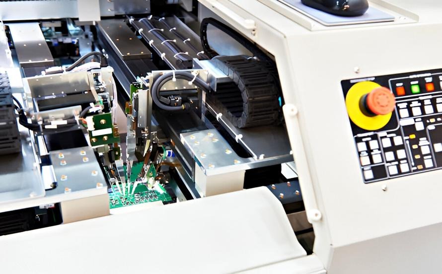
Surface Mount and Through-Hole Design Considerations
Modern PCB assemblies often combine Surface Mount Technology (SMT) and Through-Hole Technology (THT).
SMT components are mounted directly onto the board surface, while THT components use leads inserted through drilled holes.
Proper PCB Design for Assembly requires careful planning when integrating both technologies.
Designers should position through-hole components in ways that minimize interference with SMT assembly operations.
Manufacturing efficiency can often be improved by grouping similar component types together.
Understanding assembly process requirements helps optimize board layouts for both SMT and THT production.
Routing Strategies for Assembly-Friendly Designs
PCB routing affects both electrical performance and manufacturability.
Designers should avoid routing traces too close to component pads, as this may interfere with soldering and inspection processes.
Adequate spacing between conductive features reduces manufacturing risks and improves reliability.
Proper PCB Design for Assembly also considers signal integrity, power distribution, and electromagnetic compatibility while maintaining assembly-friendly layouts.
Well-planned routing simplifies fabrication and supports consistent assembly quality.
The goal is to create a design that performs effectively while remaining easy to manufacture.
Thermal Management Considerations
Heat is a major concern in modern electronics.
Improper thermal management can affect both assembly quality and long-term product reliability.
Designers should incorporate thermal relief structures where appropriate to facilitate soldering and prevent excessive heat transfer during assembly.
Component placement should also consider heat-generating devices and airflow requirements.
Proper PCB Design for Assembly ensures that thermal challenges are addressed before production begins.
Effective thermal management contributes to stable operation and improved product lifespan.
Designing for Automated Inspection
Inspection is an essential part of PCB manufacturing.
Automated Optical Inspection (AOI) systems rely on clear visibility of components and solder joints.
Proper PCB Design for Assembly supports inspection by providing sufficient spacing and minimizing obstacles that could obstruct inspection equipment.
Consistent component orientation and labeling also improve inspection efficiency.
Designing with inspection requirements in mind helps manufacturers identify defects quickly and maintain high production quality.
This approach reduces rework costs and improves overall manufacturing performance.
Testability and Access Points
Every assembled PCB should be tested before shipment.
Designers should provide adequate test points that allow manufacturers to perform electrical and functional testing efficiently.
Proper PCB Design for Assembly includes planning access for:
- In-Circuit Testing (ICT)
- Flying probe testing
- Functional testing
- Debugging procedures
Without sufficient test access, verifying product performance can become difficult and expensive.
Testability considerations should be incorporated early in the design process rather than added as an afterthought.
Common Design Mistakes That Affect Assembly
Several design mistakes can create assembly challenges.
Examples include:
- Incorrect footprints
- Insufficient component spacing
- Poor panelization
- Inadequate test access
- Thermal imbalance
- Improper solder mask design
- Misaligned connectors
These issues often result in increased manufacturing costs and lower production yields.
Following Proper PCB Design for Assembly guidelines helps avoid these common problems and supports efficient production.
Future Trends in Assembly-Oriented PCB Design
As electronics continue to evolve, assembly-oriented design practices are becoming increasingly important.
High-density interconnect boards, advanced semiconductor packages, flexible circuits, and miniaturized components require more sophisticated design approaches.
Artificial intelligence and automated DFM software are helping engineers identify manufacturability issues earlier in the design process.
Digital manufacturing technologies are also improving collaboration between designers and production teams.
These advancements will continue to enhance manufacturing efficiency and product quality in the future.
Conclusion
Proper PCB Design for Assembly is a critical factor in achieving efficient manufacturing, high product quality, and long-term reliability. By considering component placement, spacing, pad design, routing, thermal management, inspection requirements, and testing access during the design phase, engineers can significantly reduce production challenges and manufacturing costs. Assembly-friendly designs support higher yields, faster production, and improved product performance across a wide range of industries. As electronic products become increasingly complex, adopting best practices for manufacturability will remain essential for success. Companies that prioritize Proper PCB Design for Assembly and work with experienced providers offering comprehensive PCB Design and Assembly capabilities can achieve more reliable products and smoother production processes.